Friday, September 17, 2010

TESTI

Discuss, Definition and Terms. 5pts each

1.Bits and Bytes.-

A BIT, is a BINARY DIGIT. A bit can be a zero or a 1 These collections of bits can represent binary numbers.
They can also represent decimal or other number systems. A binary number made of eight bits, such as 11001010 is known as a BYTE.
Four bits, such as 1101 is known as a NIBBLE (half a byte and a joke).
Sixteen bits numbers are a WORD.

2. Microprocessor System Diagram

The CPU can put a binary number on the address bus, to select an individual register in the ROM or ram or the I/O.
The arrows on this bus show that addresses go one way only.Data at the selected address can be put on the data bus.
The CPU can also put data on this bus which can be written into a register of ram or i/o.
It is not possible to write data into ROM (read only memory).
This is shown by the single arrow on the ROM data bus and double arrows on the other two.The control bus instructs the chips to do various things, such as when to read or write etc.The clock tells all the chips when to change what they are doing.

3. ALU All arithmetic and logical instructions are carried out by the ALU.an eight bit instruction informs the ALU which operation it is to carry out.One number to be manipulated comes from the accumulator, the other from memory or another register.The result is stored in the accumulator.Flags in the status register are set to indicate the result, such as negative etc.

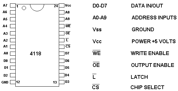
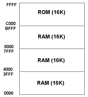
4. ROM
Memory chips are simply a collection of registers , each with its own address.Data, in the form of 0's and 1's, is stored in the registers.ROM chips can be read from, but not written to.They are non volatile, which means that they retain their contents after power is removed.Most ROMs are programmed during manufacture of the chips.Others, PROGRAMABLE ROMS, PROMS, can have their contents programmed in after manufacture.The 2716 ROM shown above is an EPROM.

5. Instructions and Programs

Instructions are represented by binary numbers called operational codes, or OPCODES.
They are frequently written in hexadecimal.

Different CPU's have different instructions.

ex .ADD add to the contents of the accumulator.
STA store the contents of the accumulator.
LDA load into the accumulator.
TAX transfer the contents of the accumulator to register X.

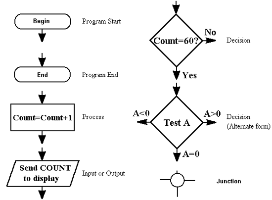
A program is a list of instructions, usually written using mnemonics.

Here is the sequence of events for writing programs.

Define the problem.
Produce an algorithm (a list of instructions, written in everyday language).
Produce a flow chart.
Write the program using mnemonics.
Assemble into hex opcodes. (an assembler is a program which does this).
Test by running the program.
DEBUG IT !!

6.Flow Chart Symbols

Flow Chart Symbols


When planning software, one of the stages is to produce a flow chart.The shape of the box indicates its function.Further data is given as text inside the box.

7. Interrupts

Interrupts Tutorial

Interrupts

The microprocessor system may be measuring temperatures in the Sahara desert.Once a year it receives a radio signal telling it to stop measuring temperatures and send all last year's data to base.
This is an INTERRUPT.
The CPU completes it current instruction. It then pushes any data it wishes to save onto the stack.
It then jumps to a routine which services the interrupt.Once the interrupt routine is completed, it pulls the saved data from the stack and carries on measuring temperatures
There are two pins on the CPU which, when taken low, cause a hardware interrupt.
RQ can be sensed or ignored depending the value of the interrupt flag in the status register.NMI cannot be ignored.

8. System Flags
The 6502 CPU contains a status register and each individual bit is a FLAG.

A flag indicates the result of the previous operation.

N result is negative
V result too big, causing an overflow
B set by software BRK command
D in decimal mode
I an interrupt has occurred
Z result zero
C carry

The flags are tested by the CPU and, depending on their state, determine which part of the program the CPU will jump to.

9. Buses
A bus is a collection of wires.Diagram A is a four bit bus.

Zeros and ones can be put on the bus, 0 volts for zero and +5 volts to represent a one.

The smallest number that can be put on a four bit bus is 0000.
The largest is 1111 which is 15 in decimal and F in hex.
Therefore sixteen different numbers can be placed on this bus, 0000 being the lowest and 1111 the highest.

Rather than draw four wires, we use the representation shown in diagram B.
Many micoprocessor systems use a eight bit data bus.
The smallest number that can be placed on it is 00000000.
The largest number is 11111111 which is equivalent to 255 in decimal.
Therefore 256 different numbers can be placed on this bus.
255 in decimal is FF in hex. A sixteen bit bus is shown in diagram C.
The smallest number we can put on this bus is 0000000000000000.
The largest number is 1111111111111111 which is 65535 in decimal.
Therefore 65536 different numbers can be put on this bus.
65535 in decimal is FFFF in hex.
All the registers in the memory chips have their own individual addresses, like house numbers in a street.
By putting its address, in binary, on an address bus we can select any individual register.
Address buses are commonly 16 bits, so we can select any one of 65536 registers.

10. System Clock

The clock is a square wave generator whose frequency is controlled by a crystal.

In a typical control system it oscillates at 1MHz (1 million times a second) and controls the speed at which the system operates.

The 6502 CPU has two clock signals, phase 1 and phase 2.

11. 6502 CPU

The 6502 CPU has a 16 bit address bus and an 8 bit data bus.

It is powered by a 5 volt supply.Interrupt requests tell the CPU to stop processing its present program and jump to another.The reset pin is taken low to initialize the CPU when it is first powered on.The read/write pin is taken low when writing to memory, and high when reading from it.

The 6502 has eight addressing modes telling the CPU where data is located.

12. RAM

Random Access Memory (RAM) Tutorial

Random Access Memory

RAM means random access memory.
A better name would be read/write memory.

Ram is VOLATILE, meaning that when you switch off, the data it contains is lost.

There are two main types of ram, static and dynamic.

Static ram uses flip-flops to store bits, and so consumes current whether they are storing a 1 or a 0.

Dynamic ram uses capacitors to store charges and use less power.
However, these stored charges leak away and have to be continually REFRESHED which makes the circuitry more complicated.

The 4118 is an 8 bit x1k static ram having an 8 bit data bus, D0-D7.

Data can be written to, or read from memory, depending the state of the WE pin.

There may be several memory chips, so only one is selected at a time by taking the CS pin low.

13. Memory Maps

Memory Map


.The memory map shows how addresses have been allocated for memory and any other devices connected to the address bus.Here ram has been given the lowest 48k of addresses and ROM the highest 16k.Each area of memory can be subdivides into pages of 256 addresses.Page zero occupies addresses 0000 to 255 in decimal or 0000 to 00FF in hex.

14. Fetch/Execute

The fetch/execute cycle is the process of fetching an instruction from memory, decoding it and then executing it.

The program counter in the CPU contains the address of the next instruction to be fetched.

The instruction is represented by a binary number, called an opcode.

Data (called the operand), for the instruction to work on, is at the address following that at which the instruction is stored.
If the opcode is ADD and is stored at address 10011000, then the data, eg. 10, will be stored at 10011001.

The following actions are taken during a fetch/execute cycle to fetch the opcode and operand.

Fetch opcode (read memory).
Increment program counter.
Fetch operand (read memory).
Increment program counter.
Execute instruction.

15.Addressing Modes and stacks.


When running a program, the CPU firsts loads an instruction.It then processes data using this instruction.Addressing modes tell the CPU where to find the data.The 6502 has several addressing modes.A sample is given below.IMMEDIATE addressing.In the program, the data follows the instruction.
ADD 99
Add 99 to the contents of the accumulator.

ABSOLUTE addressing.
In the program, the 16 bit address of the data follows the instruction.
STA 1243
Store the contents of the accumulator at address 1243.

ZERO PAGE addressing.
In the program, the instruction is followed by an 8 bit address.
This means that only addresses 0-255 (in page zero) can be used.
CMP 230
Compare the contents of the accumulator with the contents of address 0230.

Other addressing modes are

IMPLIED
RELATIVE
ACCUMULATOR
INDEXED
INDIRECT

TESTII

Essay. 2opts

1. Discuss and illustrate the Basic Microprocessor System/Microcontroller Block Diagram, As we shall see, much of the work performed by the CPU involves reading from and writing to memory. There are three busses involved in accessing memory: the address bus, the data bus and the control bus. The function of each of these busses is illustrated, discuss also the step by step accessing of busses into memory in a one whole sheet of paper.

ans.

A system is made up of the basic functional blocks. The Central Processing Unit (CPU) is the microprocessor and can be thought of as the system's brain. Memory, input ports and output ports are connected to the microprocessor through an address bus, a data bus and a control bus. Ports are physical interfaces through which data is sent to and from external peripherals such as keyboards, displays.


A microprocessor has three basic elements.
The ALU performs all arithmetic computations, such as addition, subtraction and logic operations (AND, OR, etc). It is controlled by the Control Unit and receives its data from the Register Array.


The Register Array is a set of registers used for storing data. These registers can be accessed by the ALU very quickly. Some registers have specific functions - we will deal with these later.

The Control Unit controls the entire process. It provides the timing and control signals for getting data into and out of the registers and the ALU and it synchronizes the execution of instructions (we will deal with instruction execution at a later date).


ReadCycle

The steps involved in the read cycle are:

  • CPU places address on address bus.
  • Control signals memory - address on address bus is valid.
  • Memory chip fetches data from location specified by the address and places on the data bus.
  • Control signals CPU - data on data bus is valid.
  • CPU takes data from data bus

Write Cycle

The steps involved in the write cycle are:

  • CPU places address on address bus.
  • Control signals memory - address on address bus is valid.
  • CPU places data on the data bus.
  • Control signals memory - data on data bus is valid.
  • Memory chip takes data from data bus and places it in the location specified by the address.


Basic Microprocessor System/Microcontroller Block Diagram


As we shall see, much of the work performed by the CPU involves reading from and writing to memory. There are three busses involved in accessing memory: the address bus, the data bus and the control bus.


Read Cycle

The steps involved in the read cycle are:

  • CPU places address on address bus.
  • Control signals memory - address on address bus is valid.
  • Memory chip fetches data from location specified by the address and places on the data bus.
  • Control signals CPU - data on data bus is valid.
  • CPU takes data from data bus

Write Cycle

The steps involved in the write cycle are:

  • CPU places address on address bus.
  • Control signals memory - address on address bus is valid.
  • CPU places data on the data bus.
  • Control signals memory - data on data bus is valid.
  • Memory chip takes data from data bus and places it in the location specified by the address.


An embedded system is made up of the basic functional blocks shown above. The Central Processing Unit (CPU) is the microprocessor and can be thought of as the system's brain. Memory, input ports and output ports are connected to the microprocessor through an address bus, a data bus and a control bus. Ports are physical interfaces through which data is sent to and from external peripherals such as keyboards, displays.


Three Basic Elements of a Microprocessor


A microprocessor has three basic elements, as shown above. The ALU performs all arithmetic computations, such as addition, subtraction and logic operations (AND, OR, etc). It is controlled by the Control Unit and receives its data from the Register Array.

The Register Array is a set of registers used for storing data. These registers can be accessed by the ALU very quickly. Some registers have specific functions - we will deal with these later.

The Control Unit controls the entire process. It provides the timing and control signals for getting data into and out of the registers and the ALU and it synchronizes the execution of instructions (we will deal with instruction execution at a later date).


I


Flo

w Chart Symbols Tutorial


.


Arithmetic / Logic Unit Tutorial


Monday, August 23, 2010

CT 411 MICROPROCESSOR SYSTEM


The address bus is the set of lines that carry information about where in memory the data is to be transferred to or from. No actual data is carried on this bus, rather memory addresses, which control the location that data is either read from or written to, are sent here. The speed of the address bus is the same as the data bus it is matched to.


The following simulation helps students understand the concepts of random access memory and the read and write cycles.

When you start the simulation you will be presented with the CPU on the left of the screen and the memory matrix on the right, with the address bus (blue), data bus (green) and the control bus (red) in between.

Initially, memory is filled with random data, as are the address and data busses.

If you refresh the page you will notice the data changes - this simulates powering down and then powering up the system.

When the student starts the read cycle by clicking on Read he/she must first choose an address to read from and then click on CPU requests data.

Notice the data begins to settle on the address bus. This is done in a very orderly fashion (one hex digit after another), which of course is not realistic. However, it is hoped that this will demonstrate to the student that it takes a finite amount of time for the address to settle on the address bus.

The student now plays the part of the control bus by clicking on:
control signals memory: address on bus is valid ->
However, if he/she signals memory too early (before the address has settled) then the wrong location is accessed.

Once the location has been selected by RAM the student plays the part of the control bus by clicking on:
<- control signals CPU: data on bus is valid
Again, if he/she doesn't wait for the data in memory to appear on the data bus, random data is read by the CPU.


the CPU with the program counter and the instruction register on the left of the screen, ROM on the right and the address bus (blue), data bus (green) and the control bus (red) in between.Refreshing the page, which simulates power-down followed by power-up, does not change the contents of ROM because ROM is nonvolatile.


However, the data on the busses at this point is random.

Step through the simulation by clicking on Next ->.

  1. The contents of the program counter are placed on the address bus.
  2. Control signals ROM: address on bus is valid ->.
  3. ROM selects location.
  4. ROM places data in location onto the data bus and <- Control signals CPU: data on bus is valid.
  5. Data on bus is placed in the instruction register.
  6. Cycle repeats at step 1 above.

Thursday, July 22, 2010

CT 411 MICROPROCESSOR SYSTEM


The address bus is the set of lines that carry information about where in memory the data is to be transferred to or from. No actual data is carried on this bus, rather memory addresses, which control the location that data is either read from or written to, are sent here. The speed of the address bus is the same as the data bus it is matched to.


The following simulation helps students understand the concepts of random access memory and the read and write cycles.

When you start the simulation you will be presented with the CPU on the left of the screen and the memory matrix on the right, with the address bus (blue), data bus (green) and the control bus (red) in between.

Initially, memory is filled with random data, as are the address and data busses.

If you refresh the page you will notice the data changes - this simulates powering down and then powering up the system.

When the student starts the read cycle by clicking on Read he/she must first choose an address to read from and then click on CPU requests data.

Notice the data begins to settle on the address bus. This is done in a very orderly fashion (one hex digit after another), which of course is not realistic. However, it is hoped that this will demonstrate to the student that it takes a finite amount of time for the address to settle on the address bus.

The student now plays the part of the control bus by clicking on:
control signals memory: address on bus is valid ->
However, if he/she signals memory too early (before the address has settled) then the wrong location is accessed.

Once the location has been selected by RAM the student plays the part of the control bus by clicking on:
<- control signals CPU: data on bus is valid
Again, if he/she doesn't wait for the data in memory to appear on the data bus, random data is read by the CPU.


the CPU with the program counter and the instruction register on the left of the screen, ROM on the right and the address bus (blue), data bus (green) and the control bus (red) in between.Refreshing the page, which simulates power-down followed by power-up, does not change the contents of ROM because ROM is nonvolatile.


However, the data on the busses at this point is random.

Step through the simulation by clicking on Next ->.

  1. The contents of the program counter are placed on the address bus.
  2. Control signals ROM: address on bus is valid ->.
  3. ROM selects location.
  4. ROM places data in location onto the data bus and <- Control signals CPU: data on bus is valid.
  5. Data on bus is placed in the instruction register.
  6. Cycle repeats at step 1 above.


hi